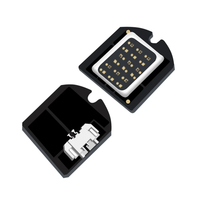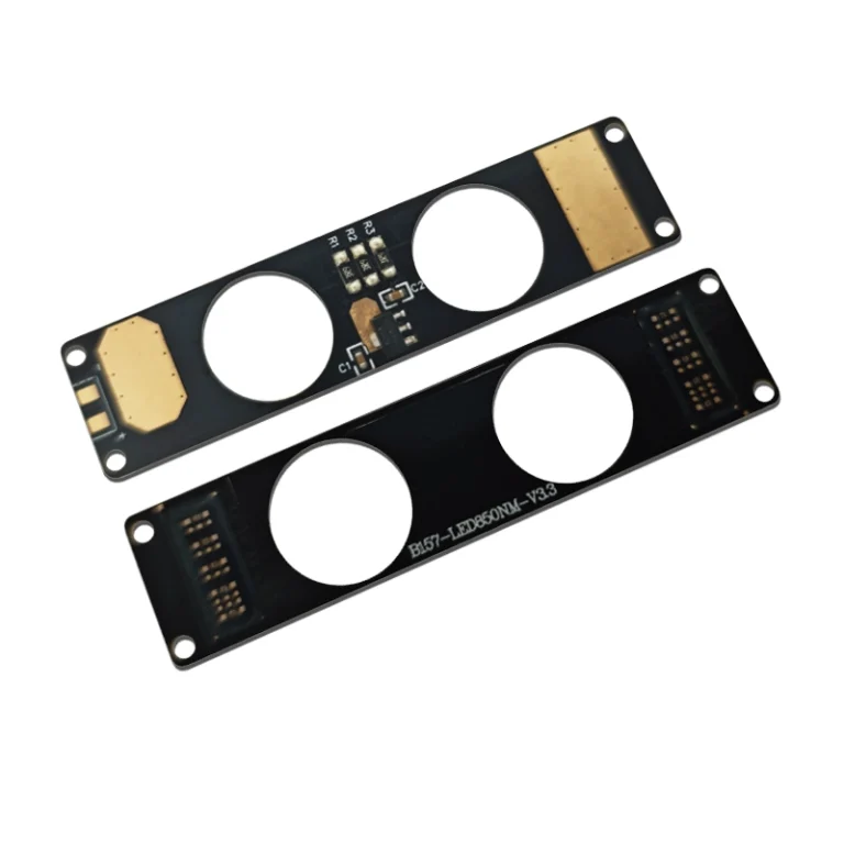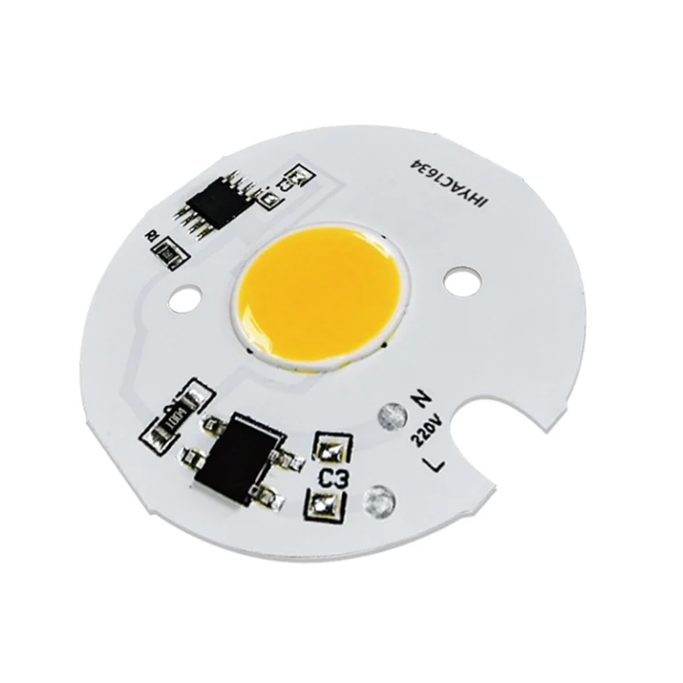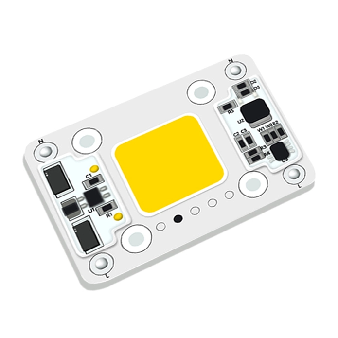




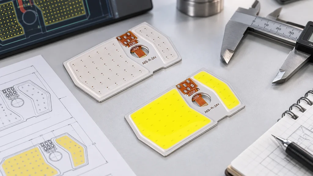
A custom COB light engine. Works or fails before the first board even gets to the LED test fixture. The PCB layout needs to turn electrical needs into something that can actually be made—copper, dielectric, components, connectors and the shape of the whole assembly. The aim is a board that moves current the way it should allows assembly makes inspection and rework possible and fits the manufacturing process that has agreed on.
This guide is about PCB layout and design for manufacturing. It does not go over the parts choosing drivers or calculating junction temperatures. These topics are already covered in COB design and heat management guides. Instead this guide looks at the choices that need to be made before sending out the Gerber files.
Start the Layout with Mechanical and Process Constraints
Begin with a constraint drawing, not component placement. Define the finished outline, keep-outs, mounting points, optic envelope, thermal-interface footprint, wire exit, component-height limit, and assembly process. These boundaries determine whether the schematic can become a buildable light engine.
An integrated PCB can hold the COB source along with driver ICs, passive components, protection devices and connectors. IHY Lighting explains that LED modules combine COBs and the supporting electronics on a PCB. This means the optical, power, control and service interfaces all need to fit within a space. At the time the design must not affect how well the module can be assembled.
- Lock the light-emitting surface and optical center before routing power or signals.
- Reserve true mechanical clearances around screws, clips, reflectors, lenses, housings, and dispensing tools.
- Confirm whether the assembler needs panel rails, tooling holes, fiducials, breakaway tabs, or defined board orientation.
- Separate component courtyard clearance from the larger access space required for soldering, probing, inspection, and connector mating.
Partition the Board by Function
A compact light engine still needs to show zones. Separate the source, the high-current path, the switching or driver area, the low-level controls and the external connections. Clear partitioning cuts down on routing confusion. Makes the planned current flow and assembly order easier to check.
Place the loop that carries the current first and keep it as short as possible. The switching nodes should take up the space they need and must not extend under sensitive controls or connector pin areas. Reviewers should be able to trace the current from the input through any protection or regulation components to the COB and back again without any blockages or unnecessary turns.
Design Copper for Current Density, Not Only Trace Width
Trace-width calculators are only a starting point. Current density rises at neck-downs, pad entries, sharp transitions, via bottlenecks, and copper interrupted by holes or keep-outs. Review the full path at its narrowest effective cross-section.
Use pours or broad tracks where practical and taper them into device pads. Avoid abrupt transitions, and geometrically balance parallel paths expected to share current. State copper thickness explicitly in the fabrication drawing rather than assuming the supplier will infer it from power.
- Calculate the worst-case current path using operating current, tolerance, transient conditions, and expected ambient temperature.
- Check voltage drop from input connector to the COB terminals, including vias and component pads.
- Keep solder-mask dams and copper-to-edge spacing compatible with the fabricator’s registered process capability.
- Avoid using decorative copper or copper logos where they can unbalance current spreading or confuse optical inspection.
Use Thermal Vias as a Manufacturable Structure
Thermal vias can connect a heat-spreading pad to more copper, but DFM depends on the stack-up and assembly method. The board-level question is whether the pattern can be drilled, plated, filled or tented, assembled, and inspected without solder loss or uneven seating.
Do not place uncontrolled open vias inside a solderable thermal pad because solder can wick into the barrels. Specify capped and filled via-in-pad, resin-filled vias, or a pattern outside the primary solder area. Match hole size, pitch, annular ring, copper weight, and fill requirement to the approved fabricator.
| Layout feature | DFM risk | Release requirement |
| Open via in pad | Solder wicking and variable joint thickness | Specify filling/capping or move vias outside the solderable area |
| Dense via field | Drill registration and resin-fill cost | Confirm minimum pitch, hole size, and fill process with the fabricator |
| Copper under mounting hardware | Shorting or damaged dielectric | Define plated/non-plated holes, washers, keep-outs, and chassis isolation |
| Large exposed pad | Voiding and board float during reflow | Coordinate paste-window design, stencil thickness, and acceptance criteria |
Place Connectors for Assembly and Service
Connector placement is mechanical, electrical and production driven. Locate connector placement where the cable can enter without crossing the aperture, fasteners, sharp housing features or tall components. Verify the envelope latch motion bend radius and pulling force not only the footprint.
Keep high-current pins close to the intended power path to avoid neck-downs and long returns. Use clear polarity or channel markings and physical keying when available. Test points should remain accessible on the assembled module without contacting the optical surface.
- Leave soldering-iron or selective-solder nozzle access for through-hole terminals.
- Keep edge connectors and wire pads away from breakaway tabs and depaneling stress zones.
- Define strain relief in the product assembly; do not expect copper pads alone to carry cable loads.
- Check connector availability, approved alternates, mating-cycle needs, and height tolerance before design freeze.
Apply Assembly-Aware Component Placement
Keep polarized parts consistently oriented where possible and leave reference designators readable. Do not trap small passives between tall components, connector walls, and the COB source; nozzles, cameras, probes, and rework tools need access.
Confirm the mixed COB and surface-mount assembly sequence early. Protect the light-emitting area from flux, paste, coating, cleaning chemistry, and handling. Define protected regions and allowable residues, while keeping fiducials and inspection targets visible when required.
Build the DFM Package Before Gerber Release
A release package should let the fabricator and assembler quote the intended product, not a generic approximation. PCB data, BOM, assembly drawing, fabrication notes, and acceptance criteria must agree; conflicting dimensions or unmarked special processes invite inconsistent interpretations.
- Fabrication drawing: stack-up, material family, finished thickness, copper weight, surface finish, hole table, tolerances, routing method, and special via treatment.
- Assembly drawing: polarity, connector orientation, protected optical areas, component-height limits, adhesive or thermal-interface boundaries, and inspection notes.
- Manufacturing data: Gerbers or ODB++, NC drill files, centroid data, BOM with approved alternates, stencil requirements, and panelization constraints.
- Verification plan: continuity and polarity checks, current and voltage test conditions, visual criteria, connector fit, and any fixture interface.
Before mass production, request a documented DFM review of deviations from standard process. Prototypes should validate paste behavior, flatness, connector access, fixture contact, optical protection, depaneling, and repeatable assembly as well as electrical operation.
Common PCB Layout Failures in Custom COB Modules
Costly layout errors are often small: a mounting hole through a return pour, an inaccessible connector latch, an exposed via that drains solder, or a copper neck carrying full module current. Also check test-point access, polarity, silkscreen under pads, edge clearance, and tolerances tied to one ideal process.
Use a cross-functional review with the mechanical model, fabrication limits, assembly flow, and test concept. Electrical approval alone is not DFM sign-off.
Conclusion
A reliable custom COB light engine PCB is organized around controlled flow, manufacturable thermal connections, accessible connectors, clear mechanical boundaries and complete release data. Treat these as linked decisions: moving a connector can change copper density via placement, test access, panel arrangement and cable strain.
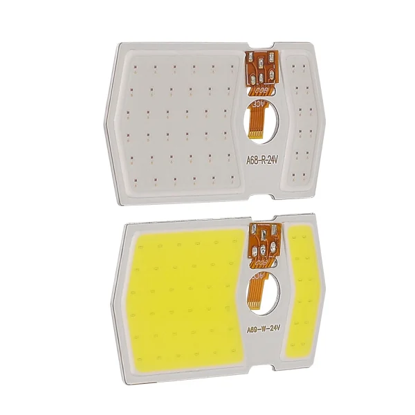
IHY Lighting offers an integrated LED module portfolio that includes board shapes, electrical designs, aluminum‑PCB formats, FPC options and connector configurations. If you need custom project you should give IHY Lighting the board envelope, input conditions, current, COB or channel requirements, connector and cable details, mounting method, optics constraints, quantity and any available drawings.
The engineering team can then review PCB integration and manufacturing fit before the layout is released.
For related system-level decisions, use the COB LED thermal-management guide for the thermal model and the COB versus CSP comparison for architecture selection. To start a board-level fit check, contact the IHY Lighting engineering team with your mechanical drawing and electrical requirements.
FAQs
Should a custom COB module use an aluminum PCB?
Aluminum PCB is often used in high-power LED modules.. The choice depends on several factors. These include the complexity of the circuit insulation needs, thickness, mechanical design, assembly process and the entire thermal path. It is important to confirm the stack-up with both the light-engine designer and the fabricator.
How should trace width be selected for a COB LED board?
Start with worst‑case current, copper thickness, permitted voltage drop, temperature rise and fabrication tolerance. Then inspect neck‑downs, pad entries, vias, holes and split pours , because the narrowest effective section normally controls density.
Are thermal vias always required?
No. Their need depends on substrate construction and the intended heat path. When used, the via structure and solder-control method must be specified; an uncontrolled open via in a solder pad can reduce assembly consistency.
Where should the power connector be placed?
Place it where the cable can mate, bend, and receive strain relief without interfering with optics, fasteners, high components, depaneling features, or test access. Keep its current path direct and verify the full mated connector envelope.
What files should be sent for a PCB DFM review?
Send fabrication data, drill files, stack-up and material requirements. Send assembly drawings, BOM, centroid data, connector and mechanical models. Send panel constraints, test requirements and notes, for vias, optical protection or tolerances.