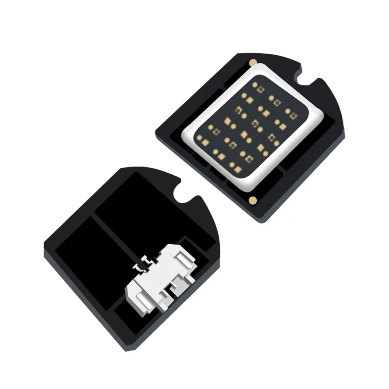


In recent years, COB (Chip-on-Board) technology has made important breakthroughs in the field of small-pitch LED displays. By directly packaging LED chips on PCB (printed circuit board), the traditional SMD (surface mount device) single lamp bead packaging step is eliminated, achieving significant performance improvement and application expansion. This article will analyze in detail the core advantages, challenges and future development prospects of COB technology in the field of small-pitch LEDs.
1. The core advantages of COB technology in small-pitch LEDs
COB technology directly packages chips, eliminating the physical gap between lamp beads in the SMD process, making the pixel pitch smaller (up to P0.5 and below), meeting the needs of ultra-high-definition display (such as 8K resolution). The lamp-free packaging structure makes the luminous surface smoother, effectively reduces moiré and granularity, and improves the close-up viewing experience. The chip is directly fixed on the PCB and is encapsulated as a whole with epoxy resin or silicone, which enhances the vibration and collision resistance and reduces the risk of SMD lamp beads falling off. The fully enclosed structure improves dustproof, moisture-proof and anti-static performance, and is suitable for complex environments (such as outdoor, industrial control rooms, etc.). COB technology directly dissipates heat through the PCB substrate, with a shorter heat conduction path, effectively reducing chip temperature, extending life and reducing light decay. For high-brightness, high-refresh-rate small-pitch LED screens, the heat dissipation efficiency of COB technology is particularly important. After eliminating multiple SMD process links, the production process is simplified, and it is expected to reduce the overall cost after scale-up. The optimization of packaging materials (such as solid crystal glue and phosphor) can further improve the consistency of light efficiency.
2. Challenges faced by COB technology
The COB process has strict requirements on the accuracy of PCB substrates, solid crystal equipment and packaging materials, with high initial investment costs and high technical barriers. The maintenance cost is relatively high, and the entire module needs to be replaced if a single chip is damaged. Traditional SMD technology is mature and the industrial chain is complete, and it still dominates the market with a pitch above P1.0. Emerging technologies such as Micro LED and Mini LED may form long-term competition with COB.
3. Application prospects of COB technology in the small-pitch LED market
COB has gradually replaced SMD in scenes with strict requirements on picture quality and reliability, such as control rooms, radio and television studios, and medical displays. The penetration of COB has been accelerated in high-end commercial scenarios (such as conference rooms and command centers) due to the demand for seamless splicing and low blue light. COB is one of the mainstream solutions for Mini LED backlighting, and it may transition to Micro LED through chip miniaturization in the future. Combined with mass transfer technology, COB is expected to play a key role in the mass production of Micro LED. Upstream chip manufacturers (such as Sanan, Huacan), packaging companies (Nationstar, Ruifeng) and terminal display manufacturers (Leyard, Unilumin, Xida) jointly promote COB standardization. The localization of equipment (such as Xinyichang die bonding machine) will reduce production costs and accelerate the popularization of technology.
4. Summary
COB technology, with its high density and high reliability, is driving small-pitch LED displays to develop towards smaller pitches and wider application scenarios. Although it faces cost and process challenges in the short term, with the collaborative innovation and large-scale production of the industrial chain, COB is expected to become one of the mainstream technical routes for small-pitch LEDs, and will be deeply integrated with Mini/Micro LED technology in the future to further expand the boundaries of the ultra-high-definition display market. For manufacturers, seizing the opportunity to layout during the window of technology iteration will determine their competitiveness in the high-end display market.